- Double-Sided PCB[2]
- FPC[10]
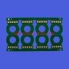
- Multilayer PCB[10]
- Other PCB & PCBA[10]
- Rigid PCB[9]
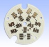
- Single-Sided PCB[3]
- Contact Person : Mr. Ho Justin
- Company Name : Shenzhen HTWY Technology Co., Ltd.
- Tel : 86-755-86315155
- Fax : 86-755-86315117
- Address : Guangdong,Shenzhen,Forsafe Science&Technology Building,Gaoxin Nan 1 st Road,High-tech Park, Nanshan District, Shenzhen City, Guangdong Province. China
- Country/Region : China
- Zip : 518052
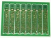
single layer PCB/single sided pcb electronics design


Related Product Searches:single layer PCB/single sided pcb electronics design,High Quality,electronics design, single layer PCB,single layer PCB
HCC PCB CRAFT ABILITY INTRODUCTION
Surface Finish HASL,Immersion Gold,Flash Gold,Gold Plating,OSP,Immersion Tin etc
Layers 1-28
Minimum Line width 3mil
Minimum Line space 3mi
Min space between pad to pad 3mil
Minimum hole diameter 0.10 mm
Min bonding pad diameter 10mil
Max proportion of drilling hole and board thickness 1:12.5
Max size of finish board 23inch*35inch
Rang of finish baord’s Thick 0.21<-7.0mm>
Minimun thickness of soldermask 10um
Soldermask:Green,Yellow,Black,Blue,White,Red,transparent photosensitive,,soldermask,Strippable soldermask
Minimum linewidth of Idents 4mil
Min Height of Idents 25mil
Color of silk-screen White,Yellow,Black
Date file format GERBER FILE and DRILLING FILE,PROTEL SERIES,PADS2000 SERIES, Powerpcb SERIES,ODB++
E-Testing 100% E-Testing High Voltage Testing
Material for PCB High Tg Material;High Frequence(ROGERS,TEFLON,TACONIC ,ARLON),Halogen-free Material)
Other test mpedance,,Testing,Resistance,,Testing, Microsection etc.
Special technological requirement Blind & Buried Vias and High Thickness copper
single layer PCB/single sided pcb electronics design