Products
- Double-Sided PCB[2]
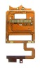
- FPC[10]
- Multilayer PCB[10]
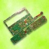
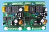
- Other PCB & PCBA[10]
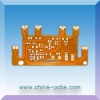
- Rigid PCB[9]
- Single-Sided PCB[3]
Contact Us
- Contact Person : Mr. Ho Justin
- Company Name : Shenzhen HTWY Technology Co., Ltd.
- Tel : 86-755-86315155
- Fax : 86-755-86315117
- Address : Guangdong,Shenzhen,Forsafe Science&Technology Building,Gaoxin Nan 1 st Road,High-tech Park, Nanshan District, Shenzhen City, Guangdong Province. China
- Country/Region : China
- Zip : 518052
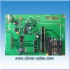
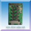
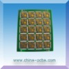
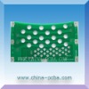
4-layer PCB with Impedance Control and 1mm Minimum Trace Size


Product Detailed
Related Categories:Other PCB & PCBA
Related Product Searches:4-layer PCB with Impedance Control and 1mm Minimum Trace Size,High Quality,PCB, pcb board,PCB001
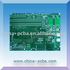
1 Circuit electronic board PCB
2 One-stop service: design, PCB fabrication, PCB Assembly,
3 Testing, housing, turnkey, etc
Related Product Searches:4-layer PCB with Impedance Control and 1mm Minimum Trace Size,High Quality,PCB, pcb board,PCB001
Key Specifications/Special Features:
Thickness: 1.6mmMinimum trace size: 0.1mmMinimum drill: 0.15mmBlind and buried holesLayer: 4-layerBoard finished thickness: 0.2 to 7.0mmMaterial: FR-4Maximum finished board sizes: 150x 180mmMinimum hole size: 4mil (0.1mm)Minimum trace width/space: 3mil/3milCopper thickness: 0.5 to 6ozCopper thickness in hole: >18umInner packing: vacuum packing/plastic bagOutline tolerance: ±0.13mmHole size tolerance: PTH: ±0.076mmNPTH: ±0.05mmWith UL and TS16949:2002 marksSpecial requirements: impedance control,Profiling: punching, routing, V-cut and bevelingProvides OEM services to all sorts of printed circuit board assembly as well as electronic encased productsPrimary Competitive Advantages:
Electronic LinkExperienced StaffGuarantee/WarrantyPriceProduct FeaturesProduct PerformancePrompt DeliveryQuality ApprovalsReputationServiceSmall Orders AcceptedMain Export Markets:
Eastern EuropeNorth AmericaCentral/South AmericaAsiaWestern EuropeAustralasia4-layer PCB with Impedance Control and 1mm Minimum Trace Size
Other products